Applications | MindVision UV Industrial Camera MV-PXL90U for Scratch and Hidden Injury Inspection
Characterization and Applications of Ultraviolet Spectroscopy
UV Ultraviolet light is an invisible line of light in the electromagnetic spectrum between visible light and X-rays, with a wavelength range of 10-400 nanometers (nm). It is divided into three bands based on wavelength differences:
-UVC (100-280nm): the shortest wavelength and the highest energy, but it is almost completely absorbed by the earth’s ozone layer and cannot reach the surface.
-UVB (280-320nm): partially blocked by the atmosphere, making imaging more difficult.
-UVA (320-400nm): accounts for 95% of surface UV radiation and is the main band for UV imaging.

The retina of the human eye only perceives visible light at wavelengths of about 380-750 nm, while ultraviolet light has even shorter wavelengths (<380 nm) and therefore cannot be directly observed. Special equipment (e.g. UV cameras, fluorescent materials) is needed to convert it into a visible signal.
The UV wavelengths commonly used in the industry are 365nm and 395nm. UV cameras are widely used in high-resolution video microscopy, corona inspection, semiconductor and non-destructive testing, etc., to capture structural defects, fluorescent markers and characteristic signals of changes in substances that are difficult to detect under visible light.
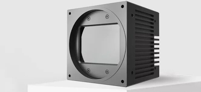
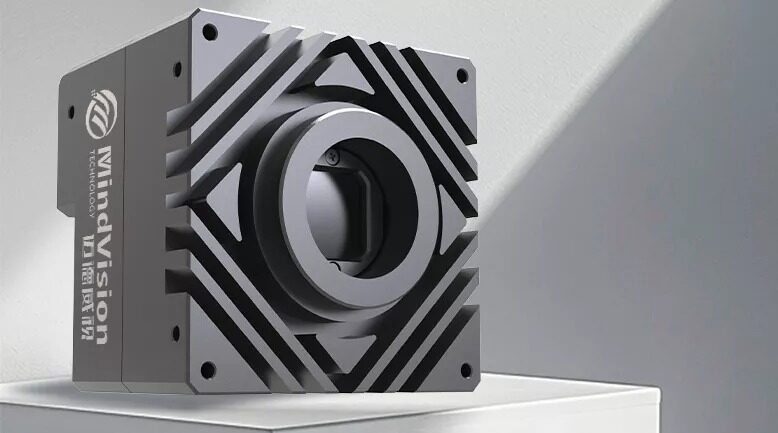
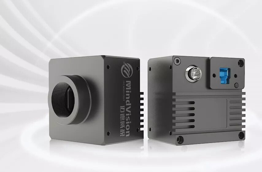
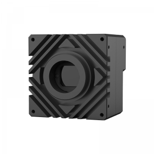
MindVision’s new UV array industrial camera, the MV-PXL90U, is designed for broad-spectrum inspection scenarios, covering a range of 200-1100nm and enhanced and optimized for the 250-380nm UV band. Its core performance includes:
– 9K Ultra-HD resolution: accurately captures microscopic defects and fluorescence signals;
– 256+32TDI technology: enhance signal-to-noise ratio and imaging efficiency in low-light environment;
– 529kHz ultra-high line frequency: to meet the needs of high-speed dynamic inspection;
– Water-cooled heat dissipation design: to ensure the stable operation of the equipment in high temperature and high load conditions.
It can be adapted to semiconductor manufacturing, material surface inspection, biological fluorescence analysis and other fields, providing reliable solutions for high-precision UV imaging.

Fine Scratch and Defect Detection
The UV image sensor utilizes the scattering effect of UV to accurately detect micron-scale pattern defects on semiconductor wafers and hidden scratches on metal surfaces. It converts damage invisible to the naked eye into high-resolution signals through grayscale contrast imaging technology, realizing non-contact detection and avoiding secondary damage to precision components.


Transparent Resin Coating Condition Inspection
UV image sensors are highly effective in detecting the uniformity of resin coatings in electronic devices. The colorless transparent resin appears black under UV imaging due to its light absorption properties, while the uncoated area appears white due to the reflection of the metal substrate. The difference in black/white contrast can quickly locate defects of thin coating, leakage, or overflow, ensuring a precise and controllable manufacturing process.

Visible Light Inspection
Looking down on protective resins

UV Inspection
Protective resin appears black
Areas of application

Industrial Inspection

Glass Dirt Detection

Biomedical